


- Home >
- Project cycle
Project cycle
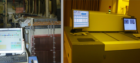
The three sites of the Cimulec-Group have modern and homogeneous industrial equipment.
The realisation of a printed circuit board requires a variety of steps. Three domains are necessary for its realisation: mechanics, optics and chemistry. The main stages in the production of your printed circuit boards are described below:
1. Sales and data processing
2. Image transfer and internal engraving
3. Stacking and pressing4. Drilling
5. Metallization and transfer external image
6. Solidification / Stripping / Engraving-
7. Varnishing and finishing
8. Electrical test and final control
-
Sales and data processing
Process description
Our sales team is specialized to meet your needs and answer your questions as soon as possible.
The CAM-Service is responsible for requests regarding technical feasibility.
It also takes care of the utility generation and generation of tools (creation of drilling programs, electrical tests ...).Know-how - Advantages of the group
We have eight workstations with GENESIS 2000 at our disposal.
It is available at both sites and thus simplifies the exchange of tools between the two sites.Remarks
Please send your documents with your specifications, if possible, in one of the following formats: Gerber, ODB +, Barco, DXF.
Adding additional information, such as a blueprint and specifications is very much appreciated. -
Image transfer and internal engraving
Process description
This process allows for direct exposure to UV rays of the tracks that are supposed to appear as copper. The parts of the layer which have been exposed are polymerized and cured. They protect the future tracks during the process of chemical etching.
Know-how - Advantages of the group
Each of our companies is equipped with a LDI.
This advanced tool offers a high degree of precision and great flexibility.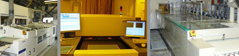
-
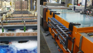
Stacking and pressing
Process description
The stratification stacks the layers accordingly to the stacking plan.
The stack is then placed in a press to be heated and cooled successively. This step removes moisture, and the solvent epoxy. Then everything is solidified.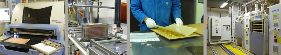
-
Drilling
Process description
The drilling aims at creating vias that will allow the establishment of a connection between the layers.
Remarks
The group has two drills that can drill 11 holes per second with high accuracy.
We are able to drill stud holes (Z controlled axis, contact-drill...). -
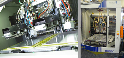
Metallization and transfer external image
Process description
The first step is to clean the vias (desmearing), because drilling leaves a residue of melted epoxy..
The second step is to deposit copper in the holes to allow an interconnection between the layers.
In a second step, the transfer operation is used to draw the external image of the circuit. -
Solidification / Stripping / Engraving
Process description
The solidification process allows thanks to an electrolytic deposit to add copper in the place, where later, the tracks are to be found. The copper is then protected by tin and lead.
Thanks to a chemical process the photosensitive film is removed (Applied in order to reproduce the design of the tracks).
The engraving removes the copper, which has not been protected by the solidification of the tin and the lead. -
Varnishing and finishing
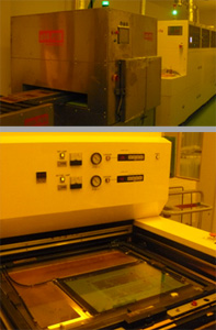
Process description
During this step the printed circuit board is coated with varnish. It protects the conductors from oxidation.
A finishing is carried out in different SMC areas and at the holes.Know-how - Advantages of the group
The companies of the group have excellent knowledge about the thickness of the varnishing.
The different finishes available are: SnPb reworked, HAL lead-free, chemical ENIG NiAu, chemical Sn, chemical silver..Remarks
The durability of the printed circuit boards depends on the processing. Depending on the type of PCB certain versions are more preferable (see link "Finishing" to learn more about it).
-
Electrical test and final control
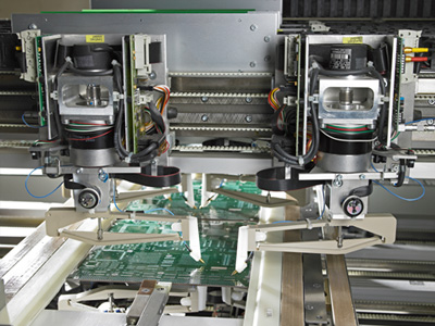
Process description
Electrical testing ensures that the printed circuit board is functional (cut traces, short circuit ...).
The final inspection verifies the documentation and physics of the printed circuit boards (dimensions, hole diameter, flatness ...).
This step enables a declaration of conformity.Know-how - Advantages of the group
4 mobile latest generation probe tester allow us to quickly test all types of printed circuit boards.
For over 20 years the group has been an IPC member and is mastering all IPC-standards perfectly.Remarks
Please send us your technical criteria for open PCBs, if they differ from the criteria of the IPC.